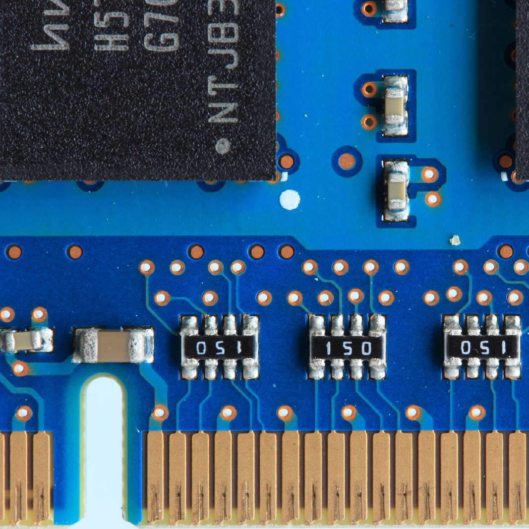
As the technology goes to higher and higher frequencies and with decreasing size in board size; Signal Integrity is an essential part of the design process especially to this modern world of electronics design.

The demand for fast devices is increasingly rising thus the rising and falling edge of the signal have to maintain when high speed devices are mounted to PCB board. The effects of the PCB layout can be detrimental in signal performance when design rules and constraints is not properly taken care of and SI must be determined upfront during the design stage.

Combining our tools in Allegro PCB SI and Adiva a well-known CAD software tools, will ensure that the PCB design layout will have a better Signal Integrity (SI) performance.


Key features:

  • Experience of handling prelayout & postlayout designs.
  • Innovative design methods in Fine Pitch Micro BGA designs.
  • Successfully executed complex Multidrop/Multipoint topologies.
  • Asserting PCB layer stackup/Layer ordering/PCB materials based on SI results.
  • Validating the logic level, Drive strengths , Termination techniques, Thresholds, Over/Under Shoot, propagation Delay, Noise margin etc., Slew rate, Timing budget (Setup/Hold time), Eye diagram
  • Design Technologies expertise – PCIe, DDRII, DDRIII, High-speed USB, Bluetooth, GPS, WLAN, SRIO, XAUI, etc.
  • In-house developed tools for QC
  • Handled up to 12GBps speed.
  • Post-Route Signal Integrity Analysis.
  • Post-Route Crosstalk Analysis.
  • Post-Route EMC Analysis

Contact us now!

Contact 080-42111685 or Leave a message.